|
|
|
|
 |
Established in late 1992 in the state of Colorado, Applied Physics, Inc. has product distribution in Europe, Asia, United States, Canada and South America. Applied Physics is known throughout Asia, Europe and the USA for providing advanced aerosol particle control, offering ingenious solutions to complex aerosol problems involving the generation, deposition, sampling and/or measurement of nano particles from 3nm to 10 µm in size. Well-conceived displays, features and interfaces are combined with advanced technology.
Link:www.AppliedPhysicsUSA.com |
|
|
|
- Product Features
- Technical Parameters
- Download
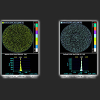
• Clearly visible as a spot, and the remaining wafer surface is left free of any deposition.
• Help to determine if a PSL Calibration Wafer is too dirty to use as a size reference standard.
• Spot Deposition forces all the desired PSL Spheres onto the wafer surface at a controlled “spot” location, thus very few PSL spheres and much higher count accuracyas aresult.
• Applied Physics uses a Model 2300XP1 with a Differential Mobility Analyzer (DMA) to ensure the NIST traceable PSL size output and count is accurate.
• A CPC is used to control count accuracy.
• Minimizes unwanted Haze, Doublets and Triplets are deposited in the background.
|
PSL and NIST SRM Particle Size Standards:100mm,150mm,150mm,200mm&300 mm Wafers,Prime Silicon
|
|
|
|
|
|